Close Form
Menu


A Printed Circuit Board, commonly called a PCB, is the structural and electrical foundation of modern electronic products. It mechanically supports components and connects them through precisely designed copper circuits. From a simple single-sided board to a high-density interconnect multilayer board, every PCB must pass through a controlled sequence of engineering, fabrication, inspection, and testing steps.
For companies looking for a custom printed circuit board or a complete printed circuit board service, understanding the production flow makes it easier to control cost, reliability, delivery time, and product performance. This guide explains the complete PCB manufacturing and assembly process, from design review to shipment.

Fig. 1 PCB manufacturing process — 13 steps at a glance
Production starts with CAM engineering. The manufacturer reviews Gerber or ODB++ files, drill data, drawings, stack-up information, impedance requirements, copper weight, surface finish, solder mask, material grade, and special tolerances. CAM engineers then prepare the panel, compensate for etching, generate exposure data, and create drilling and routing programs.
A DFM, or Design for Manufacturability, review is essential before production. It checks trace width and spacing, annular rings, solder mask openings, minimum hole size, board-edge clearance, impedance structures, and possible short-circuit risks. If a conflict is found, the engineering team should issue an Engineering Question and obtain customer approval before releasing the job.
The manufacturer cuts large copper-clad laminates into production panels. Standard FR-4 glass-fiber epoxy is widely used, while high-TG FR-4 is selected for higher thermal requirements. Aluminum PCBs support heat dissipation; PTFE laminates are used for high-frequency applications, and PI materials are common in flexible circuits. After cutting, the panels are deburred, cleaned, and identified for traceability.
For multilayer boards, inner-layer cores are first cleaned and lightly roughened to improve dry-film adhesion. A photosensitive dry film is laminated onto the copper surface. UV exposure transfers the circuit image, and developing removes the unexposed film. The exposed copper is etched away, leaving the required circuit pattern. The remaining film is stripped afterward.
Inner-layer AOI compares the manufactured pattern with the original design and detects opens, shorts, pinholes, missing copper, and line defects. This is a critical quality gate because an inner-layer defect may cause the entire multilayer board to fail after lamination. Oxide treatment then creates a uniform surface that improves bonding with prepreg and reduces delamination risk.
Multilayer lamination combines inner-layer cores, prepreg, and copper foil into one board. The materials are stacked according to the approved layer sequence and fixed with tooling pins. In a vacuum press, controlled heat and pressure soften and cure the resin in the prepreg, bonding every layer together.
After pressing, the panel is cooled and trimmed. X-ray equipment identifies inner-layer targets so that subsequent drilling can be aligned accurately with the circuit pattern. Pressing parameters must be controlled carefully because excessive resin flow, voids, or uneven pressure can affect thickness, impedance, and reliability.
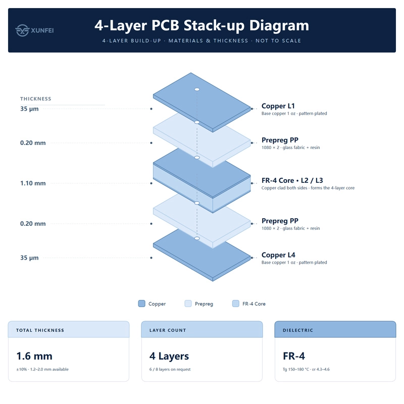
Fig. 2 4-layer PCB stack-up: copper, prepreg and core
Mechanical drilling creates standard through-holes, while laser drilling forms small blind microvias for HDI boards. X-ray alignment helps prevent registration errors between holes and inner-layer pads. Mechanical drilling can leave resin smear on the hole wall, so a desmear process is required.
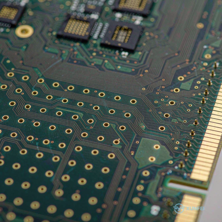
During desmear, chemical treatment removes resin residue and exposes the copper connection points. Electroless copper then deposits a thin conductive seed layer on the otherwise insulating hole wall. Electroplating thickens the copper across the panel and inside the holes. This sequence creates reliable vertical electrical connections between PCB layers.
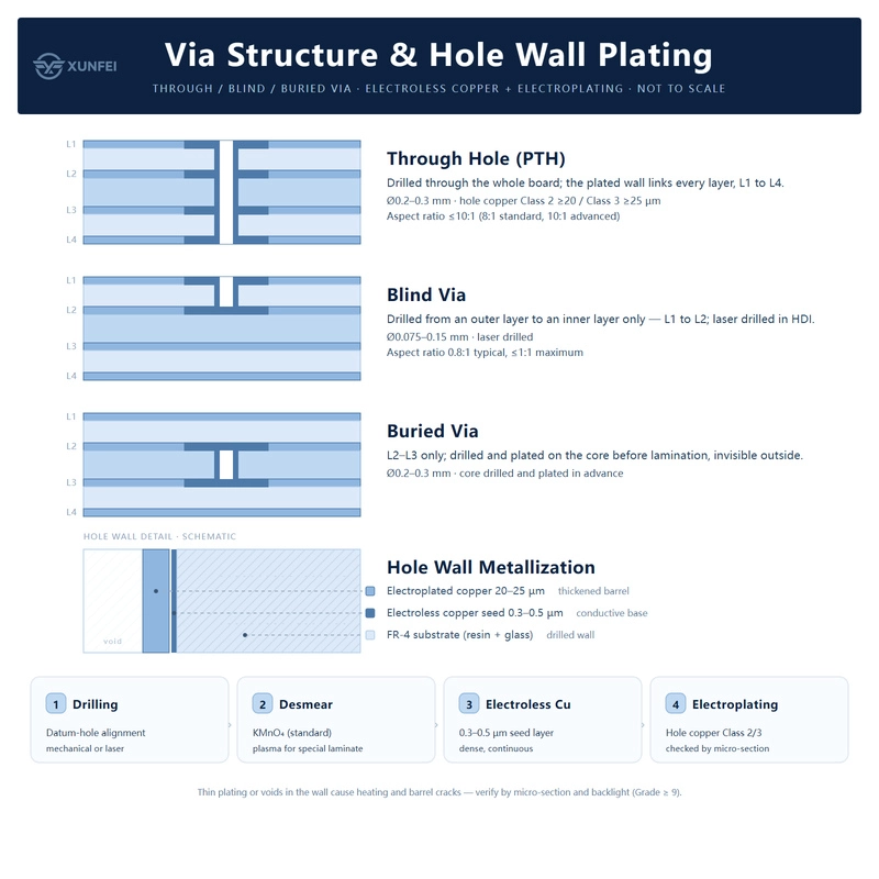
Fig. 3 Via structure and hole-wall metallisation
The outer-layer process repeats surface cleaning, dry-film lamination, exposure, and developing. Pattern plating adds copper to the circuit areas and deposits tin as an etching resist. After the dry film is stripped, unwanted background copper is etched away. The tin is then removed, leaving the finished outer-layer traces and pads. Outer-layer AOI provides another inspection gate before solder mask.
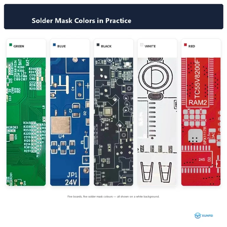
Solder mask is applied by screen printing, curtain coating, or spraying. After pre-baking, UV imaging and developing open the pads, test points, and other areas that must remain exposed. The remaining ink is cured at high temperature. Solder mask prevents oxidation, reduces the risk of solder bridges, provides insulation, and protects the copper from physical damage.
Silkscreen, also called legend, adds reference designators, polarity marks, logos, and revision information. It is printed on top of the solder mask and must not cover solderable pads or critical inspection areas.
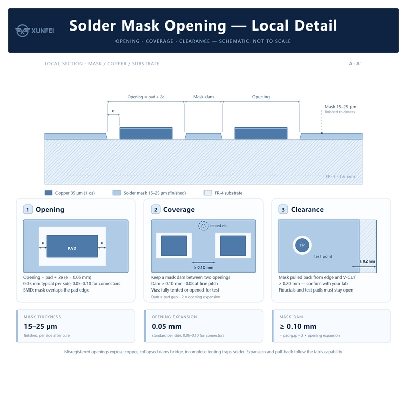
Fig. 4 Solder-mask opening in close-up: opening, tenting and clearance
Surface finish protects exposed copper pads and preserves solderability. HASL is economical and suitable for general applications, but its flatness is limited. ENIG provides a smooth surface and strong oxidation resistance, making it suitable for fine-pitch, BGA, and contact applications. Immersion silver and immersion tin offer relatively flat surfaces, while OSP is cost-effective for short storage periods. Hard gold is selected for wear-resistant connector contacts such as gold fingers.
The correct finish depends on pad geometry, shelf life, assembly method, reliability requirements, and budget. A professional PCB board manufacturer should explain these trade-offs before production.
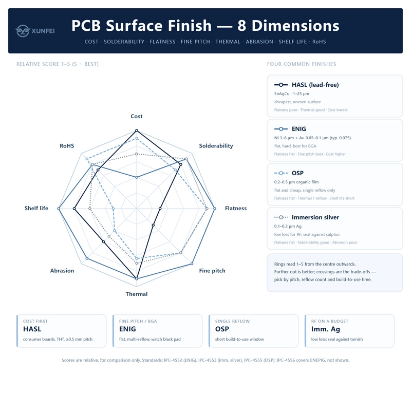
Fig. 5 Four common surface finishes compared across 8 dimensions
Routing, V-Cut, or die punching separates the finished board from the production panel. Routing is suitable for irregular outlines, V-Cut is efficient for straight board edges, and punching is often used for simple high-volume shapes.
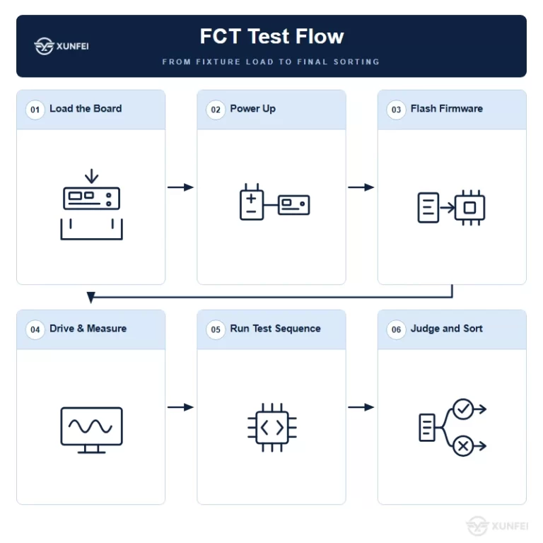
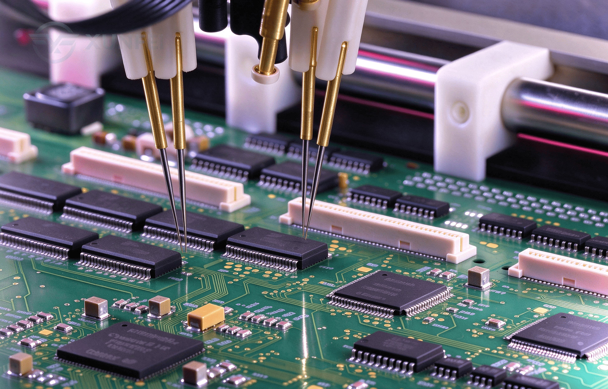
Electrical testing verifies continuity, isolation, opens, and shorts. Flying-probe testing is flexible for prototypes and small batches, while fixture testing is faster for mass production. Final quality control checks dimensions, appearance, solder mask, silkscreen, surface finish, impedance where required, packaging, and moisture protection before shipment.
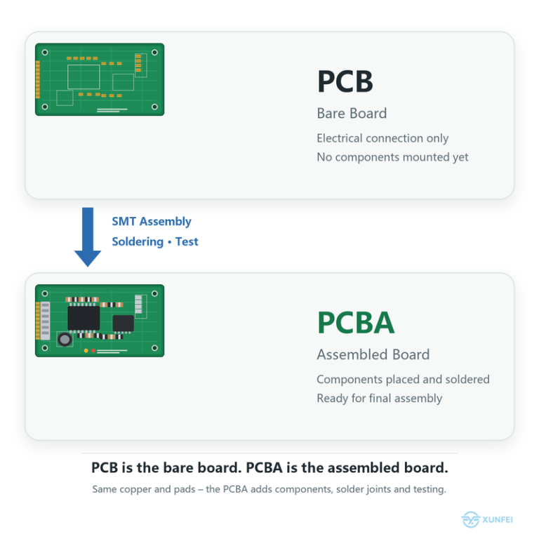
PCB fabrication produces the bare board; PCB assembly installs components and turns it into a functional electronic assembly. In SMT PCB assembly, solder paste is printed onto pads, SPI checks paste volume and alignment, and a placement machine installs components. The board then passes through a reflow oven, followed by AOI, X-ray inspection for hidden joints when necessary, and functional testing.
A reliable PCB assembly supplier should support component sourcing, custom PCB assembly, assembly design review, traceability, repair control, and production reporting. Combining pcb fabrication and assembly under one qualified partner can reduce logistics risks and improve communication.
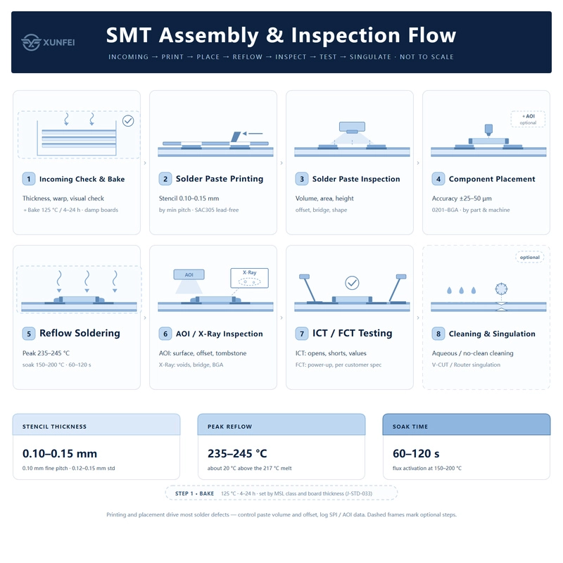
Fig. 6 SMT assembly and inspection flow
When comparing printed circuit board manufacturers, evaluate engineering support, material control, process capability, certifications, inspection equipment, traceability, delivery performance, and communication quality. Ask whether the supplier can support prototypes, low-volume production, volume manufacturing, and PCB assembly design optimization.
The best PCB assembly service is not simply the lowest-priced option. It should provide stable quality, transparent engineering communication, controlled supply chains, documented inspection standards, and practical solutions for design, fabrication, and assembly.
A dependable PCB Printed Circuit Board is the result of disciplined engineering, controlled fabrication, accurate inspection, and reliable assembly. From DFM review and material selection to lamination, plating, surface finish, testing, and SMT, every stage contributes to final product quality. Choosing an experienced partner for printed circuit board service can help reduce design risk, improve manufacturing efficiency, and accelerate time to market.
What files are required for PCB production?
Common files include Gerber or ODB++, drill files, fabrication drawings, stack-up information, pick-and-place data, bill of materials, and assembly drawings.
Which surface finish should I choose?
HASL is suitable for general cost-sensitive boards. ENIG is often preferred for fine-pitch, BGA, and higher-reliability applications. The final choice depends on design and assembly requirements.
Can one supplier provide fabrication and assembly?
Yes. A qualified supplier can provide PCB manufacturing and assembly, component sourcing, SMT, inspection, testing, and final delivery under one production plan.
How can I obtain a custom PCB quotation?
Provide the board files, quantity, layer count, material, copper weight, surface finish, delivery target, and assembly requirements. Complete information helps the engineering team quote accurately.