Menu
Resources

Resources

Home / Resources / Blog / What is PCB? Basic Knowledge & PCB Design Process

What is PCB? Basic Knowledge & PCB Design Process

Release time:09/22/2026
Share to:

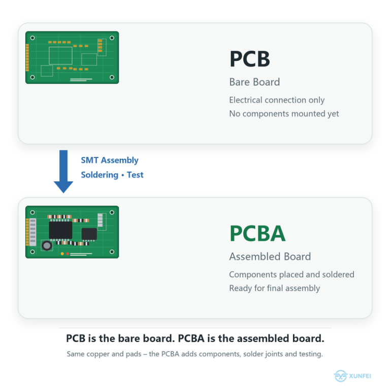
    What is PCB? 

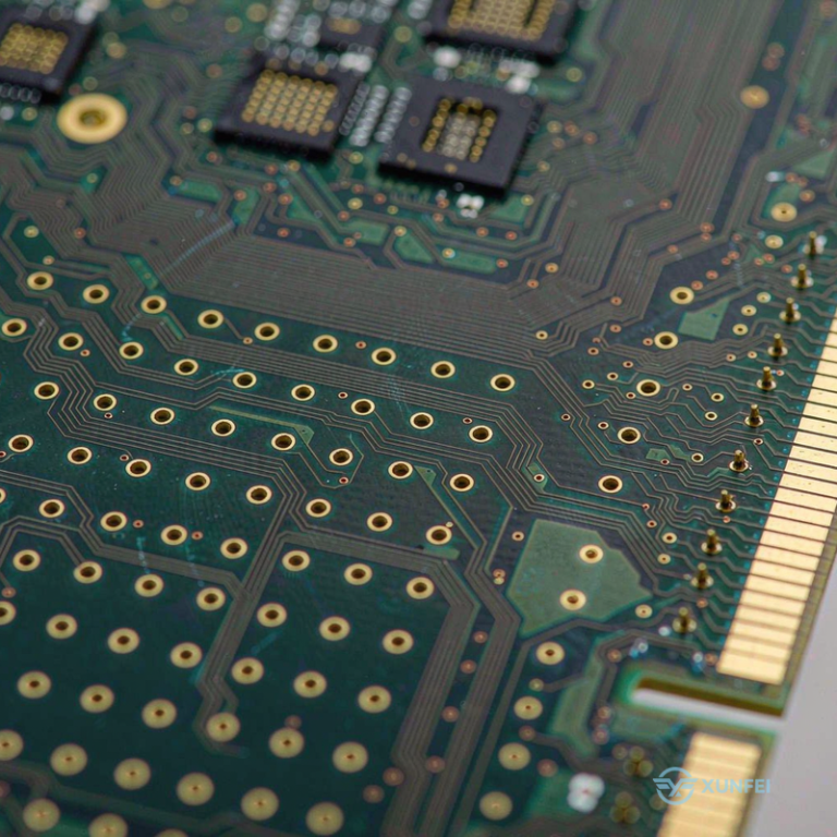
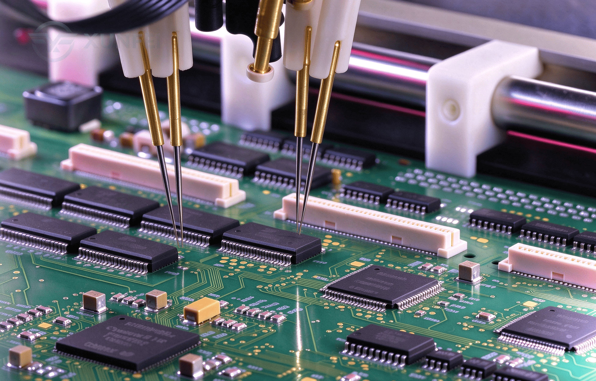
    PCB,  short for printed circuit board,  is the cornerstone of modern electronics and plays an indispensable role. From electronic watches worn daily and calculators essential to students,  to indispensable office computers, to the office of the indispensable computer, and then connected to the world of communication electronic equipment, and even a symbol of the country is military power of the military weapons system, these seemingly different, different functions of the electronic equipment, in their internal structure, are invariably embedded in a sophisticated and complex PCB board.

Types of Printed Circuit Boards

    Printed circuit boards fall into three main categories: Flexible Printed Circuits (FPC), rigid circuit boards, and Rigid-Flexible PCBs (Rigid-Flex PCB).

    Flexible Printed Circuit/FPC stands out for its high-density wiring, light weight, ultra-thinness and excellent bending properties.

    Rigid circuit boards use rigid substrates as their base. They feature a robust structure and a fixed shape, making them suitable for most electronic applications, with the benefits of lower cost and a relatively simple manufacturing process.

    Rigid-Flex printed circuit boards combine a flexible PCB with a rigid circuit board through a series of processes such as lamination. This type of board combines the respective advantages of FPC and rigid PCB; however, its disadvantages are equally obvious: complex production process, relatively low yield, production difficulties, and relatively long production cycle.

Classification of PCB

Classification according to the number of layers and copper foil distribution. 

    According to the number of layers of copper foil, circuit boards can be divided into single-sided boards,  double-sided boards and multilayer boards.


· Single-Layer Boards:  

Wires are provided on one side only. Since the wiring is confined to one side only,  there are many design constraints.  These boards were more common in early circuits,  but are now mainly used in products with simple structures and strict cost requirements.

· Double-Layer Boards:

 Wiring is provided on both sides of the board.  Thanks to the double-sided wiring,  it is possible to solve the problems caused by staggered wiring in a single panel,  thus achieving a more optimal layout.  Double-sided boards are often used in relatively simple circuits,  chip pin distribution is not dense

· Multi-layer boards:

 In order to expand the wiring area,  multi-layer boards use multiple layers of single- or double-sided sheets bonded together with insulating material. Commonly used multi-layer boards are usually between 4 and 8 layers.

Commonly used raw materials for PCB board

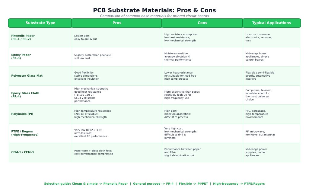
   Common classifications by substrate include:  phenolic paper laminates,  epoxy paper laminates,  polyester glass mat laminates, etc.Each of these materils has its own strengths. 

    Among many substrate materials, FR-4 boards have become the first choice in the field of high-grade electronic products such as computers and communication equipment due to their excellent performance.

    For FR-4 sheets, the industry has three core requirements: the first is flame resistance — the board must withstand high temperatures and remain non-combustible, only softening; the second is the Tg point (glass transition temperature), which reflects the material's stability at high temperatures; and the third is the dielectric constant, a parameter that directly determines the signal transmission efficiency and quality of the circuit board.

    In short, FR-4 boards for PCBs need to provide excellent flame resistance, maintain their shape at a specific temperature without burning, and offer a suitable Tg point and low dielectric constant, in order to meet the stringent requirements of modern electronic products for high performance and high stability.

Classification by the type of through holes


    Through Hole: This type of hole completely penetrates the entire electronic circuit board, with each end terminating on the outermost layer of the board.

    Blind Hole: A blind hole starts on one of the outer surfaces of the electronic circuit board, does not penetrate the entire board, and ends somewhere on the inner layer.

    Buried Via: A buried via sits completely inside the electronic circuit board, with neither end touching the outer layer of the board, and serves only to connect different layers inside the board.

To learn more about PCB holes, please refer to this blog.


Classification by surface treatment

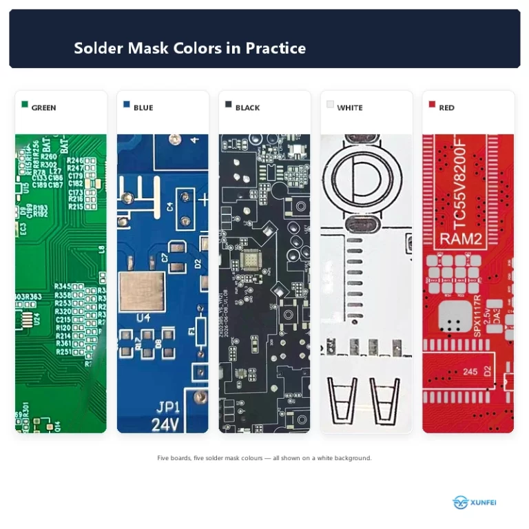
Since copper is prone to oxidisation in its natural environment, which may lead to poor soldering results, manufacturers usually apply a protective coating to the copper surface. The following are a few common types of surface treatments:

· Leaded HASL / Hot Air Solder Leveling:

Hot air leveling technology tins the copper surface in a leaded environment.

· Lead-Free HASL:

The process uses the same hot air leveling technology, but in a lead-free environment.

· Immersion Gold / ENIG:

The process deposits a layer of electroless nickel on the copper surface, then dip-plates it with gold. Immersion silver and immersion tin use similar processes, but with different materials.

· Oxidation Protection / OSP:

An organic protective film coats the copper surface to prevent oxidation.

Functions of PCB board

    Electrical Interconnection Engineers carefully lay out the copper traces on a PCB board to connect various electronic components, such as resistors, capacitors and integrated circuits, together to build a complete circuit system. This type of connection not only simplifies the circuit design process, but also significantly improves circuit reliability.

    Component Support PCBs provide a solid support platform for electronic components, ensuring that they are arranged in a tight and orderly manner. Through soldering and other processes, manufacturers firmly fix components on the PCB, thus enhancing the structural stability and portability of the equipment.

    Circuit Protection The insulating material on the PCB boards effectively shields the circuits from electromagnetic interference and protects them from external factors such as moisture and dust. This protection is critical to prolonging the life of electronic devices, especially in harsh industrial environments.

    Thermal Performance In high-performance, power-hungry electronics, where heat dissipation is a particular problem, engineers carefully design the metal layers on the PCB board, especially the copper foils, to act as efficient heat sinks. They quickly absorb and disperse the heat that the circuitry generates and prevent components from being damaged by overheating. Increasing the thickness of copper foils, optimising the layout and applying other design means can further improve the heat dissipation efficiency of PCB boards.

PCB Design Process PCB

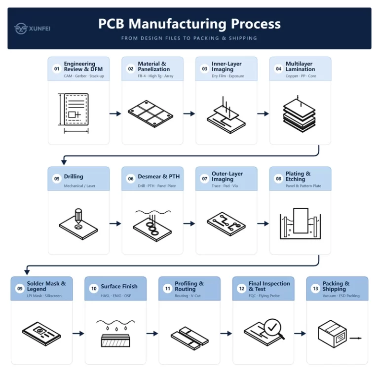
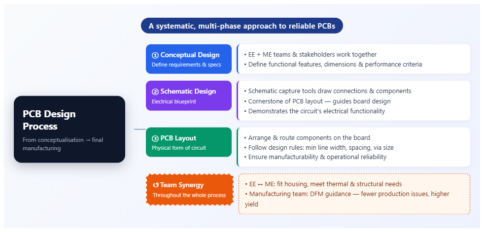
    The PCB design process is a systematic approach to creating functionally stable and reliable printed circuit boards, where every step is critical, from the initial conceptualisation to the final manufacturing of the finished product. The process consists of a number of core elements, each of which plays a decisive role in the success of the project.

    The PCB design process begins with the conceptual design phase, where the main task is to define the overall requirements and specifications of the electronic product. During this phase, the electrical engineering team, mechanical engineering team, and other relevant stakeholders work closely together to define the functional features, dimensions, and performance criteria for the PCB.

    Once the conceptual design phase is complete, the schematic design phase follows. In this phase, engineers use schematic capture tools to accurately depict the electrical connections and components of the circuit. The schematic is the cornerstone of the PCB layout, providing a clear guide to the design of the electronic circuit board and demonstrating the electrical functionality of the circuit.

    Next comes the PCB layout phase. In this step, engineers build the physical form of the circuit by carefully arranging and routing components on the board. During the layout process, they must strictly adhere to various design guidelines, such as minimum line widths, spacing, and the size of vias, to ensure the board's manufacturability and operational reliability.

    Throughout the PCB design process, the synergy between the various teams plays an important role. The electrical engineering team works in close co-operation with the mechanical engineering team to ensure that the PCBs perfectly adapt to the required housing and meet all thermal and structural requirements. At the same time, the manufacturing team provides important guidance on Design for Manufacturing (DFM), which aims to minimise problems during the production process and increase productivity.


At Xunfei Technology Co., Ltd., we offer one-stop PCB services — from Design for Manufacturing (DFM) review and rapid prototyping to volume production — helping you turn your ideas into high-quality boards quickly and cost-effectively. Contact us to start your next project.

RECOMMENDED NEWS