Understanding PCB Vias: PTH Blind Via and Buried Via
Release time:09/29/2026
Share to:
A printed circuit board (PCB) stacks layers of copper‑foil circuits upon one another, and vias create connections between different circuit layers. The principle behind this resembles the connectivity of multi‑layer underground water channels. Anyone who has played Super Mario Bros. may understand pipe‑based connectivity; yet unlike pipes that carry water, PCB vias serve electrical conduction — hence the name “via.” However, raw holes produced by a drilling machine or laser cannot conduct electricity on their own. The raw drilled‑hole surface consists only of non‑conductive resin. Engineers must therefore plate a layer of conductive material (usually copper) onto the surface of each drilled hole. This lets electrons travel between different copper‑foil layers.
1.There are three types of through-via vias that we often see, as follows:
1.1 Through hole
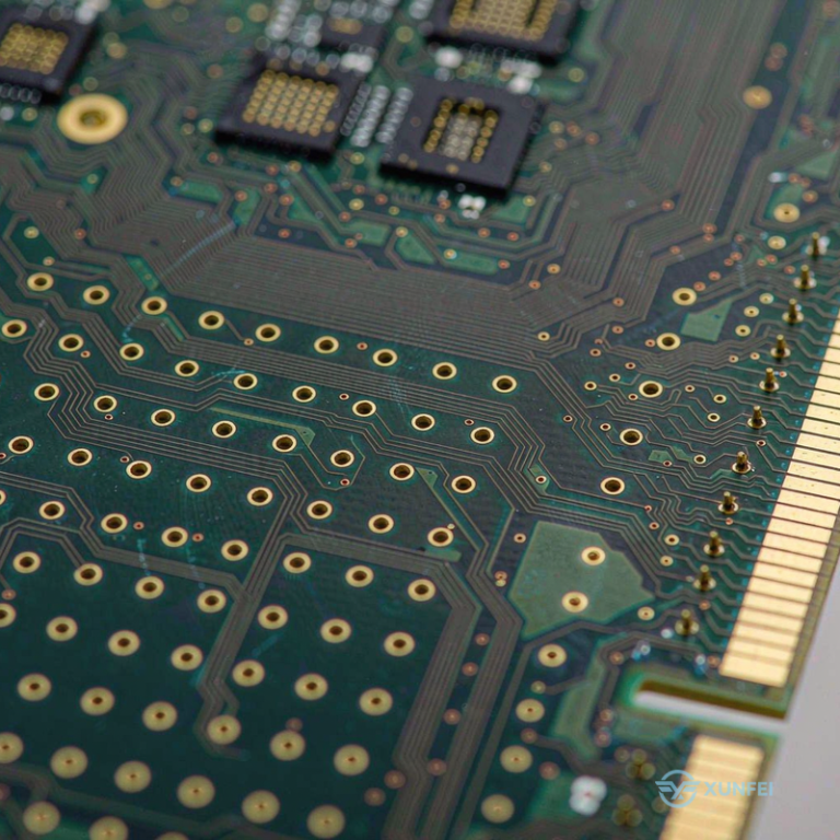
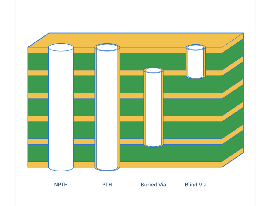
This is the most common type of via. You can identify it by holding the PCB up to a light source: plated through vias let light pass through them. Manufacturers also produce this via type most simply, because they drill or laser-cut the vias directly into the circuit board, and the process costs relatively little. In some scenarios, though, certain circuit board layers do not need connections through these PTHs. For example, imagine I own the third and fourth floors of a six-story building and want to build an internal staircase linking only those two floors. A staircase running from the first to sixth floor would waste space on the fourth floor. So even though PTHs carry low cost, they sometimes occupy extra space on the PCB.
Through Vias are also divided into PTH (Plated Through Hole) and NPTH (Non-Plated Through Hole). The former features a copper electroplated layer on its hole wall, providing electrical connectivity for soldering component pins and facilitating signal conduction. The latter has no copper plating on its hole wall and is non-conductive; it is commonly used for positioning holes and screw fastening holes.
1.2 Blind Via
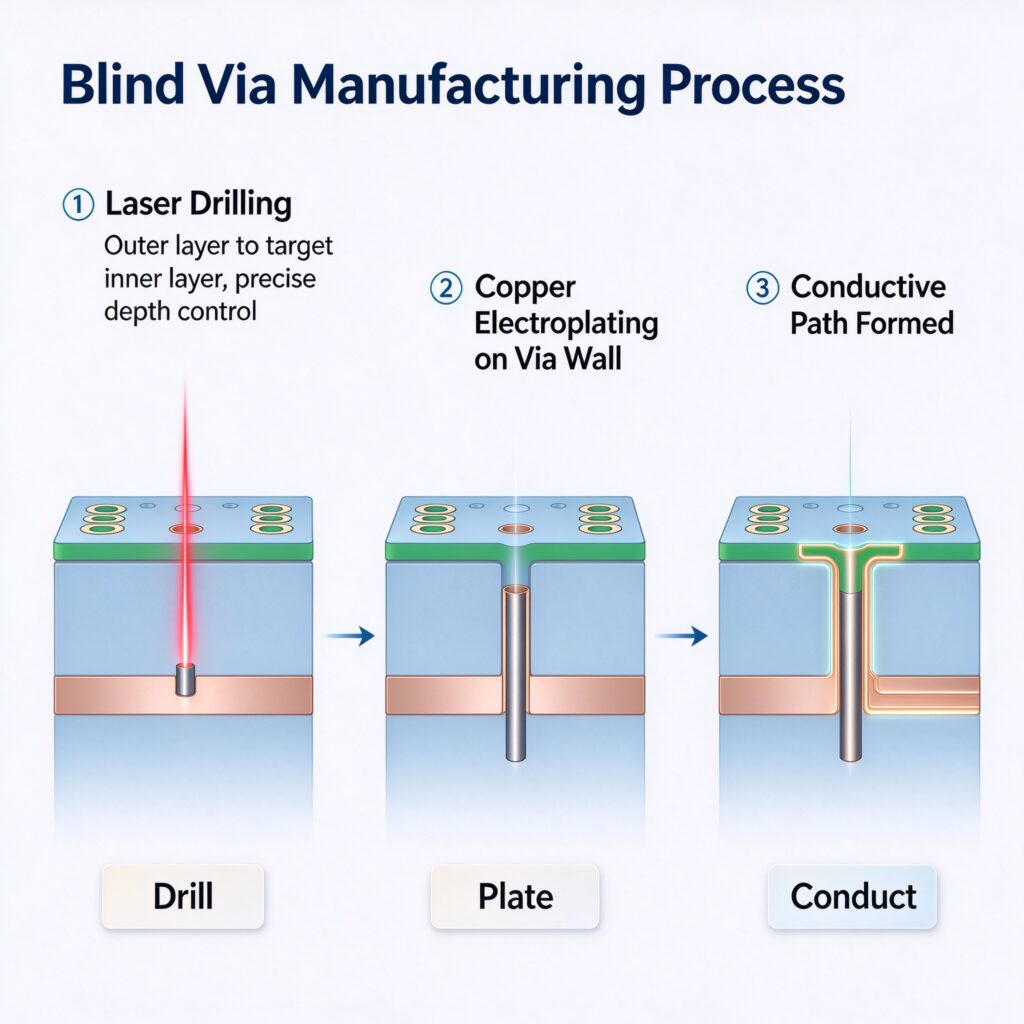
Blind vias connect the outer PCB circuit layers to adjacent inner layers through electroplated vias. You cannot see their opposite side, so engineers name them blind vias. Manufacturers adopt this manufacturing process to boost space utilization for PCB circuit layers. However, operators must pay special attention to drilling depth along the Z-axis. Poor depth control makes electroplating the inner via cavity difficult; for this reason, most manufacturers no longer rely on this drilling approach. Fabricators can also drill required connecting vias on separate circuit layers during production and then laminate all layers together in the final step.
For example, for a 2+4+2 stackup board, you can first drill the outermost two layers, or drill the 2+4 layers at the same time. This operation demands highly precise positioning and alignment equipment. Using the building analogy: in a six-story building, stairs only link the first and second floors, or the fifth and sixth floors. These structures correspond to blind vias.
1.3 Buried Via
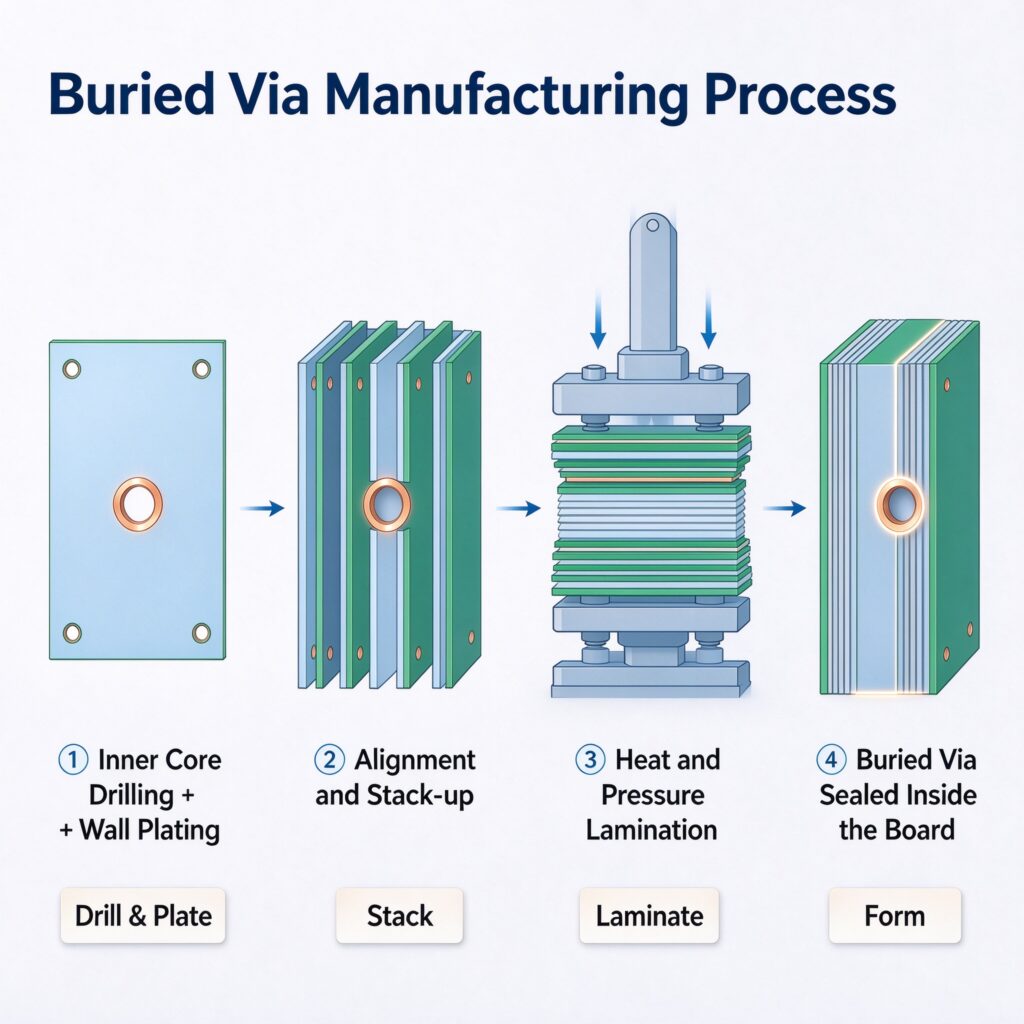
Buried vias connect two or more inner layers without reaching the outer layer. This process cannot be achieved by drilling after bonding, and requires partial bonding of the inner layers, followed by electroplating treatment, before final bonding can be completed. It is more time-consuming and expensive than making plated through vias or blind vias, and is typically used for high-density (HDI) circuit boards to increase available space for other circuit layers. Using the analogy of buying a building, when only the stairs between the third and fourth floors are connected in a six-story building, it is called a buried via. Buried vias cannot be seen from the appearance of the board and are actually located in the inner layers of the circuit board.
2. How to Manufacture Blind/Buried Via
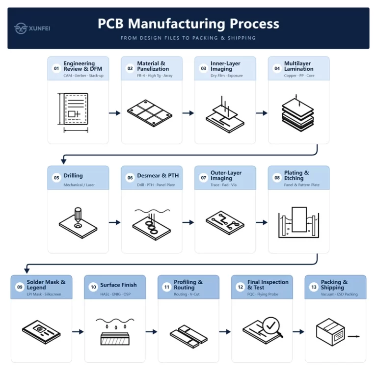
Blind and buried vias can be manufactured in two ways: before or after the multilayer lamination process. When creating blind and buried vias, one or more cores are drilled and plated through, and then the stack-up is built and compressed. More information about the manufacturing process can be found in the IPC-2221B handbook.
When creating blind vias, attention must be paid to the drilling depth. Vias that are too deep or too shallow can both have negative impacts. If the vias are too deep, signal distortion or attenuation may occur, while if they are too shallow, poor connections may result.
3. Advantage disadvantage and Considerations
Advantage
disadvantage
Considerations
Meets high-density constraints for traces and pads without increasing the total number of layers or the board size.
—
These vias must always span an even number of copper layers.
—
Both processing methods can significantly increase the cost of the circuit board, due to more complex board designs, more manufacturing steps, and more frequent testing and precision checks.
These vias cannot terminate on the top side of a core.
—
—
These vias cannot start on the bottom side of a core.
—
—
Blind or buried vias cannot start or end inside another blind or buried via unless one is completely enclosed within the other. This adds extra cost, as additional printing cycles are required.