Menu
Resources

Resources

Home / Resources / Blog / SMT Process :Surface Mount Technology industrion and process

SMT Process :Surface Mount Technology industrion and process

Release time:09/24/2026
Share to:

1.What is SMT

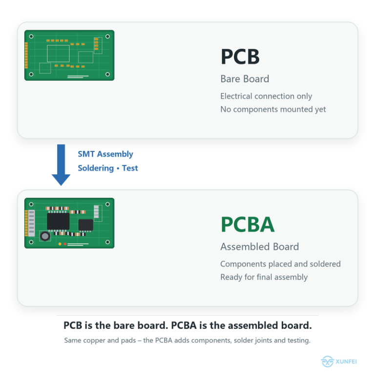
Surface Mount Technology (SMT) is a technology that attaches surface-mount components directly onto the circuit board. In the soldering process, solder paste is first printed on the circuit board pads, then the surface-mount components are accurately placed on the solder-paste-coated pads; by heating the printed circuit board until the solder paste melts and then cooling it, the connection between the components and the printed circuit is achieved.Lorem ipsum dolor sit amet, consectetur adipiscing elit. Ut elit tellus, luctus nec ullamcorper mattis, pulvinar dapibus leo.

1.2Advantages and Limitations of SMT


Advantages

Limitations

1. High assembly density. Relatively speaking, using SMT can reduce the volume of electronic products by 60% and the weight by 75%.

1. The nominal values on the components cannot be seen clearly, and maintenance work is difficult.

2. High reliability. Generally, the rate of defective solder joints is less than 10 parts per million (ppm), which is an order of magnitude lower than that of the wave soldering technology for through-hole components.

2. It is difficult to repair and replace the devices, and special tools are required.


3. The consistency of the coefficient of thermal expansion (CTE) between components and printed boards is poor. With the advent of dedicated disassembly/assembly equipment and new low-expansion-coefficient printed boards, this is no longer an obstacle to the further development of SMT.

2.basic process

The SMT process has two basic processes: one is the solder-paste reflow soldering process, and the other is the placement-wave soldering process. In actual production, the appropriate process flow should be selected according to the types of components, the production equipment used, and the needs of the product. 

1) Solder-paste reflow soldering process. Its characteristics are simple and fast, which is conducive to reducing the product size.  

2) Placement-wave soldering process. It makes use of the double-sided space of the board, further reducing the volume of electronic products, and through-hole components are still used. The price is low, but the equipment requirements are higher; the wave soldering process produces more defects and it is difficult to achieve high-density assembly.  

3) Mixed installation. This process makes full use of the double-sided space of the PCB, which is one of the ways to minimize the installation area, while retaining the low-cost characteristic of through-hole components.  

4) Solder-paste reflow soldering process used on both sides. This process makes full use of the PCB space and minimizes the installation area, but the process control is complex and strict. It is often used in dense or ultra-small electronic products; mobile phones are one of the typical products. 

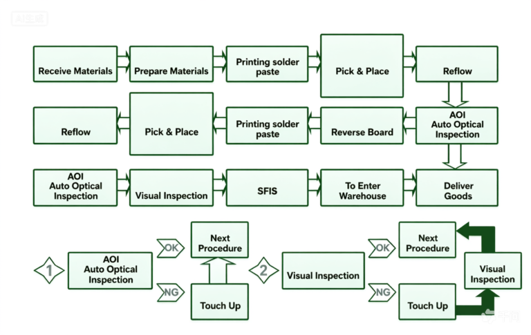
the basic process flow diagram of two layers PCB is the following:

3. setp 1 printing of solder paste

The printing of solder paste is the first process in SMT. It involves three basic elements: solder paste, stencil, and printing machine. A reasonable combination of the three is very important for achieving quantitative distribution of solder paste. The solder paste has been introduced above; this section mainly describes the stencil and the printing machine.  


 3.1 Manufacturing method of metal stencils

   Chemical corrosion method: due to side corrosion, the finish of the window wall is insufficient, and the effect on stainless steel materials is poor, so the solder-leakage effect is also poor.

    1.Laser cutting method: a microcomputer controls a CO2 or YAG laser generator to cut the window directly on the metal template, like light painting.  

    2.Electroforming method: the template made by electroforming is expensive and is suitable for products welded with fine-pitch devices.  


3.2 printing machine 

     An automatic printing machine usually has an optical alignment system. By identifying the alignment marks on the PCB and the template, it achieves automatic alignment between the template window and the PCB pad. The accuracy of the printing machine can reach 0.01 mm, but there are many types of printing machines. Process parameters such as blade speed, blade pressure, demolding speed, and the gap between the template and the PCB still need to be set manually.  


3.3 Process Steps for Solder Paste Printing

    1.Solder paste preparation: the solder paste should be refrigerated (at 0–10 °C). Before use, take it out of the refrigerator and let it return to room temperature (about 4 hours), then open the lid. Factories with suitable conditions stir it by machine and can use it after about 0.5–1 hour. It should be noted whether the viscosity and particle size of the solder paste meet the requirements of the current product (measured with a viscometer).  

    2.Install and calibrate the template; semi-automatic operation can help with alignment by CCD.

    3.Printing solder paste: the initial dosage should not be excessive. Pay attention to the environmental quality: no wind, clean, temperature 23 ± 3 °C, and relative humidity lower than 70%. 

    4.Completion and cleaning of the template.  

    5.Separation speed.  

    6.Scraper shape and materials.  

4. step2 Mounting

4.1  SMT technology summary

In SMT production, SMT technology usually refers to the accurate placement of chip components on the PCB in a certain way. This process is called "pick and place" in English, which refers to the two actions of picking and placing.  

In the past 30 years, the placement machine has developed from the early low speed (1–1.5 s/piece) and low precision (mechanical alignment) to high speed (0.08 s/piece) and high precision (optical alignment, placement accuracy ±60 μm/4σ). A high-precision automatic placement machine is a high-tech electromechanical device composed of a computer, optics, precision machinery, ball screw, linear guide, linear motor, harmonic drive, vacuum system, and various sensors. 


4.2  Structure and Functional Components of the SMT Mounting Machine

The surface of the machine can be divided into the frame, PCB transmission mechanism and support table, X/Y/Z-Q servo system, positioning system, optical recognition system, placement head, feeder, sensors, and computer operating software. 

    1.Bottom platform: supports all components and should have sufficient rigidity. 

    2.Feeder: accommodates components in various packaging forms and sends the components to the picking site. After the PCB positioning work, the PCB is supported and correctly positioned in the X and Y directions. 

    3.Placement head: takes the components and, after positioning correction, pastes the components to the set position.  

    4.Positioning system: affects the placement accuracy and placement rate. Currently, DC servo motors are generally used to drive toothed-belt ball screw drives.  

    5.Computer control system: the brain of the placement machine, the command center for all placement operations.  


4.3  Classification of SMT Machines

According to different purposes, the placement machine can be classified in different ways:  

    1.Classification by mounting method: sequential, online, simultaneous, simultaneous/online.  

    2.Classification by mounting speed (mounting rate): low speed, medium speed, high speed.

    3.Classification by price: low-end (under USD 100,000), mid-range (USD 100,000–200,000), high-end (above USD 200,000).  

5.step3 Reflow soldering

Definition and Advantages of Reflow Soldering

Reflow soldering, whose original intention is to form a solder joint by remelting the pre-placed solder surface without adding extra solder during the soldering process, has become the mainstream process of SMT. 

Compared with traditional wave soldering, reflow soldering has the following advantages:  

    1.The solder paste can be quantitatively distributed, with high accuracy, less solder heat, fewer impurities, and relatively less usage. 

    2.It is suitable for welding all kinds of high-precision and high-demand components, such as 0603 resistors and capacitors, and chip-packaged devices such as QFP, BGA, and CSP.  

    3.Fewer welding defects: the rate of defective solder joints is less than 10 × 10⁻⁶.  

RECOMMENDED NEWS