X-Ray Inspection for BGA, QFN and Hidden Solder Joints
Release time:10/20/2026
Share to:
1. What Is X-Ray Inspection?
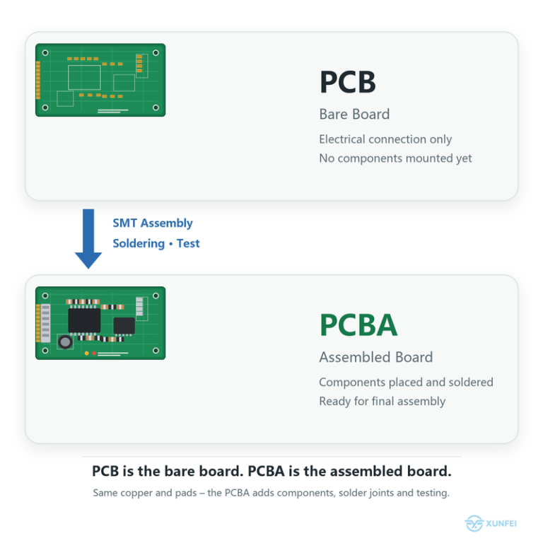
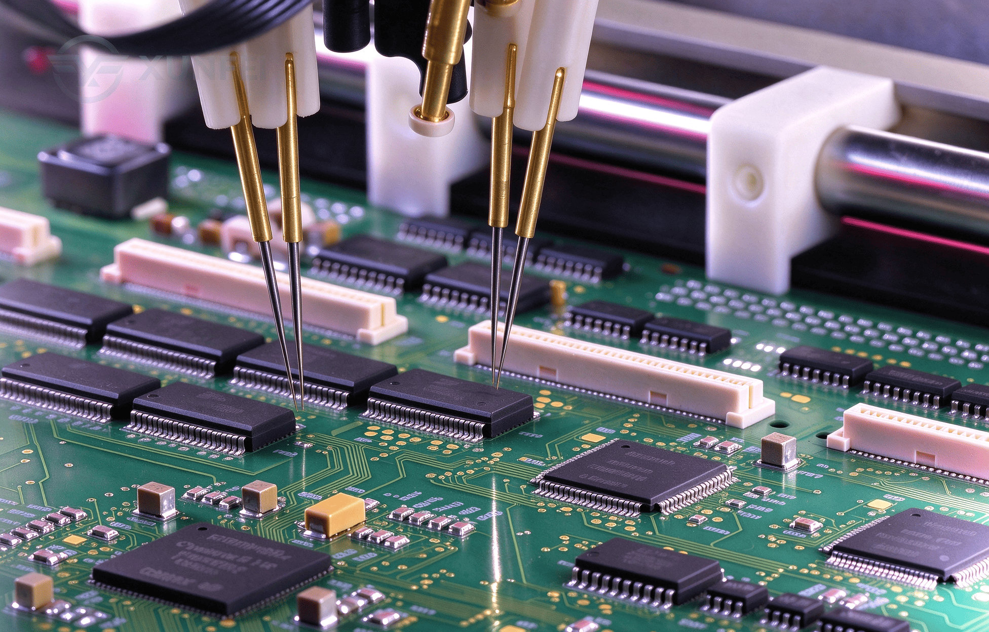
X-ray inspection works by sending X-rays through PCBA (Printed Circuit Board Assembly) boards. In doing so, it reveals hidden solder joints that optical cameras cannot see. This is why this method is critical for bottom-terminated chips—components whose solder pads or balls are located underneath the package rather than along the sides.
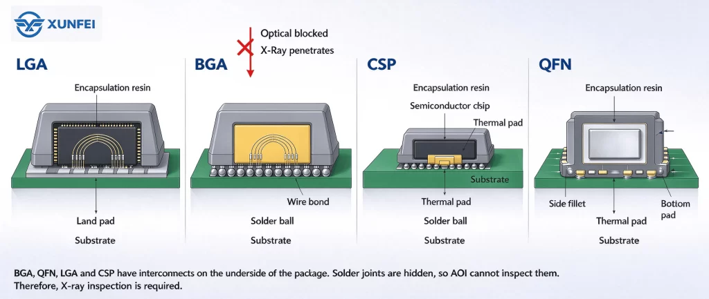
Typically, such parts include BGA (Ball Grid Array), QFN (Quad Flat No-leads), LGA (Land Grid Array), and CSP (Chip Scale Package). In these packages, the solder balls sit underneath the component packages, so AOI (Automated Optical Inspection) cannot see them-only X-ray inspection can.
2. Why Optical Inspection Cannot See BGA Solder Balls ?
BGA stands for Ball Grid Array. In this package type, the solder balls are located underneath the package body. As a result, the package itself blocks the camera's view during optical inspection.
Similarly, QFN stands for Quad Flat No-leads. In this package type, the pads are located underneath the package edge. Optical inspection can only see the side fillet of the solder joint—the visible curved surface of solder that forms along the edge—but not the full joint underneath.
Furthermore, LGA (Land Grid Array) and CSP (Chip Scale Package) suffer from the same problem: the critical joint is hidden beneath the package body, making it inaccessible to optical inspection.
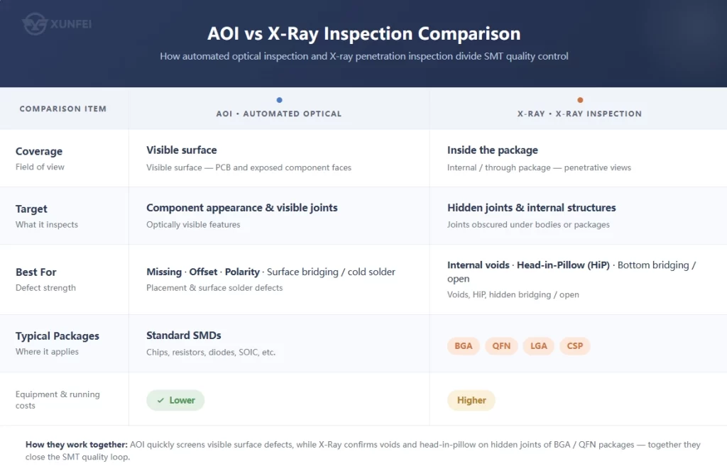
That is precisely why X-ray inspection is indispensable. Unlike optical inspection, which relies on visible light and can only examine exposed surfaces, X-ray inspection works by penetrating directly through the package body. As a result, it reveals internal solder joints invisible to the naked eye, providing a clear view of hidden connection quality.
AOI checks the surface; X-ray inspects the hidden joints. They are not competitors, but partners. AOI catches most surface defects, while X-ray captures what AOI cannot see. A complete quality system uses both.
3. How X-Ray Inspection Works ?
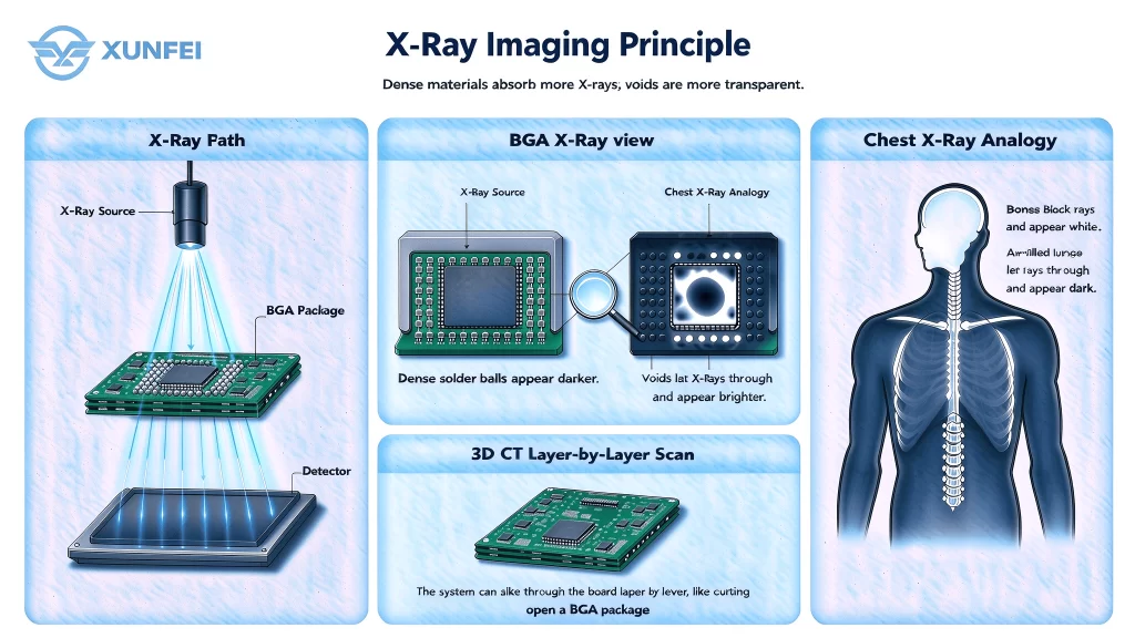
X-rays pass through the board and hit a detector on the other side. Dense material like solder absorbs more X-rays and shows up darker. Empty gaps show up brighter. It is exactly like a hospital chest X-ray. Bones block the rays and appear white on film. Air-filled lungs let rays through and appear dark.
With a 3D CT mode, the system can slice through the board layer by layer. It is like cutting open a BGA package to inspect every solder ball inside.
4. 2D X-Ray vs 3D CT
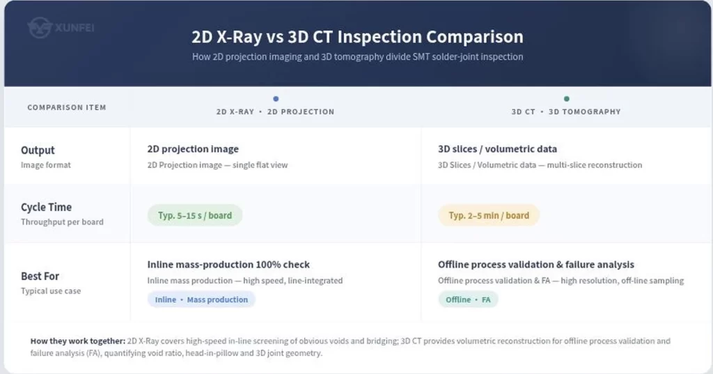
2D X-ray generates a projection image. Known for its high speed, it is ideal for inline production, effectively detecting voids, bridging, and missing balls. In contrast, 3D CT produces slice images. Although slower, it reveals the complete 3D shape of each solder joint, making it perfect for sample-level qualification and failure analysis.
5. Detectable Defects
X-ray inspection can detect a wide range of hidden defects that are otherwise difficult or impossible to identify. The key challenge is that these defects are hard to find. More specifically, they often pass visual inspection, and they may even pass ICT (In-Circuit Test)—because ICT primarily verifies electrical continuity at the time of test and cannot reliably expose marginal or latent joints.
However, such defects can fail in the field once the product is subjected to thermal cycling, vibration, or mechanical stress, which is exactly why X-ray inspection is essential for catching them before they reach the customer.
Broadly speaking, these defects fall into several categories:
Category
Defect Type
Consequences & Impact
Solder joint defects
Excessive Voids
Reduces effective contact area, weakening mechanical strength and increasing thermal resistance, leading to fatigue and cracking under thermal cycling.
Open / Missing Balls
Results in a complete loss of electrical connection, causing immediate or intermittent device failure.
Solder Bridging
Creates unintended short circuits between adjacent pads, causing functional failure or component damage.
Deformation / Collapse
Alters standoff height and joint geometry, compromising coplanarity and long-term reliability.
Package-level defects
HiP Head-in-Pillo
Solder ball and paste do not fully coalesce, leaving a latent open circuit that may fail in the field under stress.
Cracks & Die Attach Voids
Cracks compromise integrity and moisture resistance; die attach voids impair heat dissipation, leading to overheating or delamination.
Wire-bond Failures
Broken or lifted wire bonds cause open circuits, rendering the device non-functional.
6. FAQ
-What is X-ray inspection?
X-ray inspection sends X-rays through PCBA boards to reveal hidden solder joints.
-Why is X-ray inspection needed for BGA?
BGA solder balls sit under the package body. Optical cameras cannot see them.
-What is the difference between 2D X-ray and 3D CT?
2D X-ray gives a fast projection image. 3D CT gives a slower slice image with full 3D shape data.
-How long does X-ray inspection take?
About 5-30 seconds per board for 2D. About 2-5 minutes per board for 3D CT.
-Can AOI replace X-ray inspection?
No. AOI cannot see hidden solder joints under BGA or QFN packages.
Because hidden solder joint defects in BGA, QFN, LGA, and CSP packages can easily escape optical inspection, ensuring long-term reliability requires a manufacturing partner with advanced testing capabilities.At XUNFEI, we integrate our own AOI and X-ray non-destructive testing equipment into a comprehensive closed-loop production system, supported by strict pre-production DFM reviews. Request a free quote today and let us provide you with a reliable, one-stop PCB & PCBA manufacturing solution that catches critical defects before they reach your customers.