SPI vs AOI: Solder Paste and Optical Inspection in SMT
Release time:10/16/2026
Share to:
What is the difference between SPI and AOI, and do you really need both?
SPI (Solder Paste Inspection) and AOI (Automated Optical Inspection) are the two core inspection systems on a modern SMT line. They are often confused, yet they check completely different things at completely different stages.
SPI inspects solder paste right after stencil printing, before any component is placed. AOI inspects the assembled board after placement or reflow, checking component presence, position and solder joint quality. Together they form a two-layer quality system: SPI stops printing defects from ever reaching the oven, while AOI catches what happens after.
This guide explains how each system works, what defects each one can and cannot detect, how they differ, and how to use them together on your production line.
1. What Is SPI Solder Paste Inspection?
SPI means Solder Paste Inspection. It checks solder paste deposits right after stencil printing. Workers run SPI before component placement. SPI is the first quality gate in SMT production. It catches printing defects before they become soldering defects.
Solder paste printing is a critical step. If the paste volume is too low, the joint ends up with insufficient solder, causing weak joints or opens;if it is too high, excess solder can bridge adjacent pads and short the circuit. If the paste is misaligned, the component may shift during placement or tombstone during reflow. In the end, these defects all lead to the same outcome: electrical opens, shorts or intermittent contacts that cause the assembled board to fail functional test, and - if they escape inspection — field failures, customer complaints and costly rework or recalls.
1.2 How SPI Works?
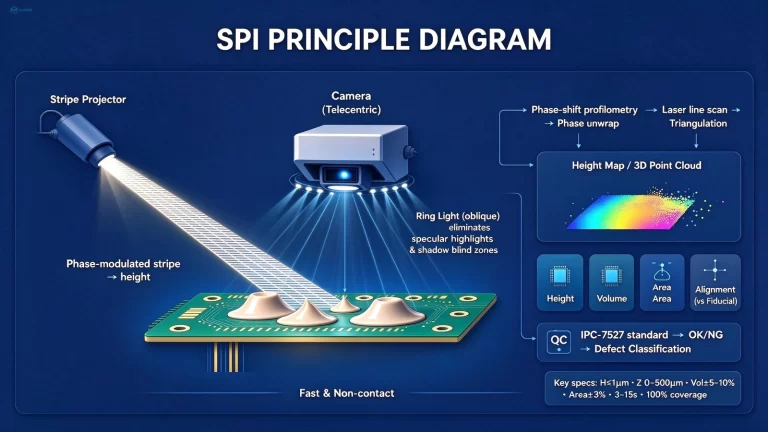
SPI uses structured light or laser triangulation. A projected light stripe falls onto the solder paste deposit. The camera captures how the stripe bends.The bending angle tells the system the height of the paste. Based on this, the system calculates volume, area and alignment.
Think of your shadow on the ground. When you stand tall, your shadow stretches long. Conversely, when you crouch low, your shadow becomes short. SPI reads the same kind of shape change.This method is fast and non-contact. It does not touch the paste or damage the board.
1.3 SPI Detectable Defects
SPI can detect a wide range of printing defects. The most common ones are:
-Insufficient paste volume → weak joints, opens, and component dropout. -Excessive paste volume → bridging and solder shorts between adjacent pads. -older paste misalignment → shifted components during placement and tombstoning during reflow. -Bridging between adjacent pads → electrical shorts that may only surface at final test. -Missing solder paste deposits → a completely open joint that no reflow profile can fix. -Paste smearing or shape distortion → voids and inconsistent joints that pass inspection but fail in the field.
None of these defects look serious on the printer. Each one, however, is a latent electrical fault waiting to happen.
-A missing deposit → an open circuit. -Bridging → a short. -Insufficient paste → a joint that survives functional test and then cracks in the customer's hands.
This is the real cost of an uncontrolled printing process: failed boards at final test, expensive rework, elevated field failures — and in the worst case, a recall. Catching these defects at the printer costs a fraction of fixing them after assembly.
1.4 SPI Value and Test Time
Some reliablestudies show that, Printing is the single largest source of soldering defects in SMT assembly. SPI catches these risks at the earliest stage - before the board reaches placement or reflow - which prevents expensive rework in later production steps.
Typical test time is 2-5 seconds per board. SPI runs at inline conveyor speed, so it does not slow down the SMT line. For high-volume production, SPI is not optional. It is a cost-saving tool.
2. What Is AOI Automated Optical Inspection?
AOI stands for Automated Optical Inspection. It is a visual quality-check technology for SMT production lines. Using optical cameras to capture surface images of PCBA, it automatically finds soldering and placement defects, and thus acts as a core quality-control step for SMT manufacturing. AOI does not touch the board. It uses light and cameras to compare real images against a golden sample.
2.1 How AOI Works?
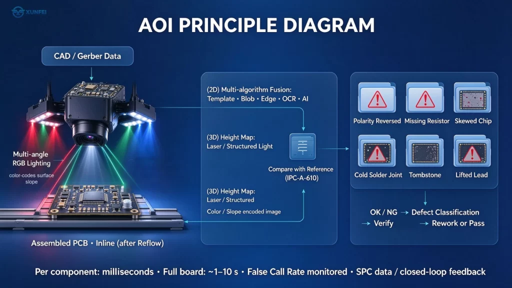
High-resolution cameras take pictures of assembled PCBs under multi-angle LED lighting. The system runs image-processing algorithms to compare the real-shot images against the golden sample, flagging any abnormal difference.
Examples include a missing resistor, a skewed chip or a cold solder joint. Think of it as an eagle-eyed inspector. The inspector compares every board side by side with a perfect reference, pixel by pixel, in milliseconds. AOI is fast and repeatable. Moreover, it does not get tired.
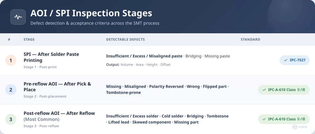
2.2 AOI Inspection Stages and Detectable Defects
AOI is deployed at three key points along the SMT production line. AOI detects visible surface defects, but it cannot inspect hidden solder joints beneath BGA or QFN packages - which is why X-Ray inspection remains essential.
2.3 AOI Applications and Test Time
Consumer electronics, automotive electronics, industrial control, medical devices and communication modules all rely on AOI. Miniaturised components, high board density and solder joints far smaller than the human eye can resolve have made AOI standard equipment on virtually every SMT production line today.
Typical inspection time is 3–8 seconds per board, depending on board size, component count and camera resolution. Because AOI runs inline, it inspects at conveyor speed and never becomes a bottleneck in the SMT line.
AOI is not a replacement for SPI — it is the second half of the same quality system. SPI inspects solder paste before components are placed; AOI inspects components and solder joints after. Each covers a stage the other cannot reach, and together they
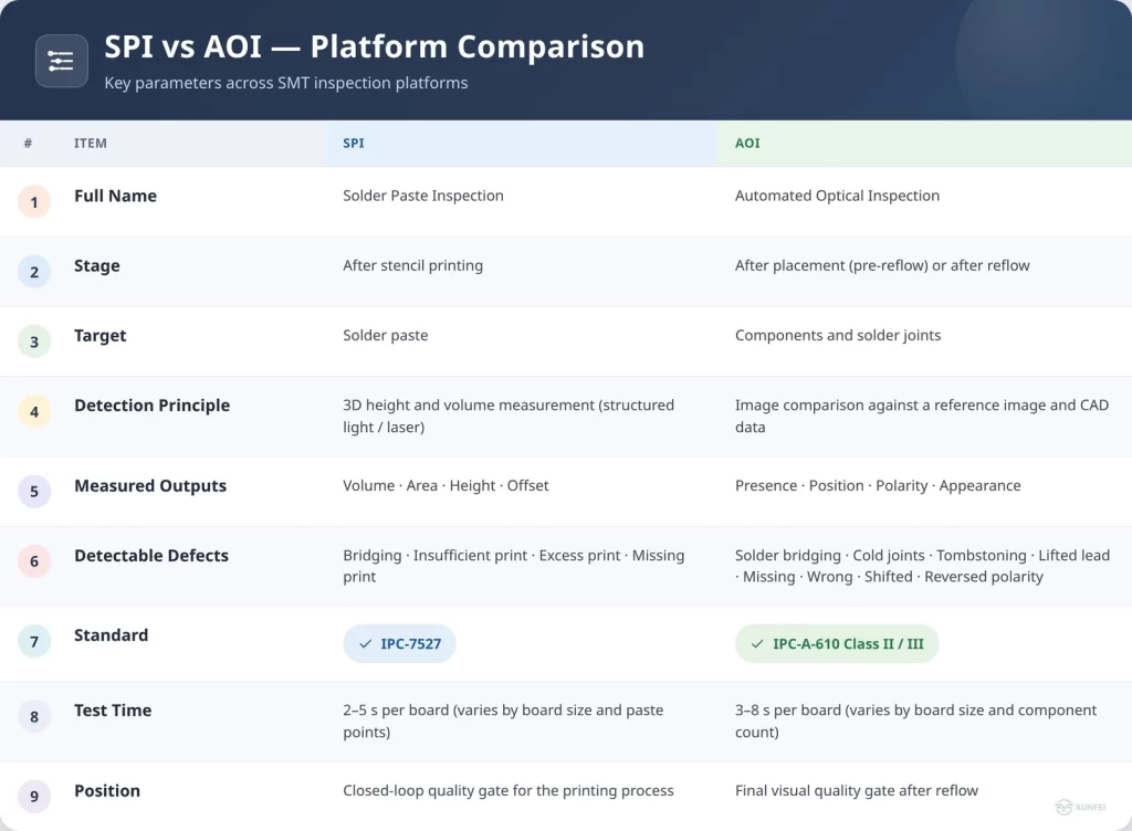
3. SPI vs AOI: Key Differences
SPI catches printing problems, while AOI catches placement and soldering problems. Therefore, both are necessary for a complete SMT quality system.
4. FAQ
-What is SPI?
SPI means Solder Paste Inspection. It checks solder paste deposits after stencil printing.
-What is AOI?
AOI means Automated Optical Inspection. It uses cameras to find placement and soldering defects.
-What is the difference between SPI and AOI?
SPI checks solder paste. AOI checks components and solder joints. SPI runs earlier in the line.
About 3-8 seconds per board, depending on board size and camera resolution.
Nearly 30 years in electronics manufacturing, ISO 9001 and RoHS certified, and fully compliant with IPC standards — the quality system behind every board we build.
Our SMT lines run automatic AOI and X-Ray inspection as standard equipment, and every order passes a pre-production DFM review, so defects are caught — and designed out — before they cost you money.
Send us your Gerber files today and get a free DFQ assessment from an engineer with over 10 years of experience.
Lorem ipsum dolor sit amet, consectetur adipiscing elit. Ut elit tellus, luctus nec ullamcorper mattis, pulvinar dapibus leo. Request a Free Quote