Via-in-Pad (VIP) PCB Introduction: Manufacturing Process, Design Rules and Advantages
Release time:10/09/2026
Share to:
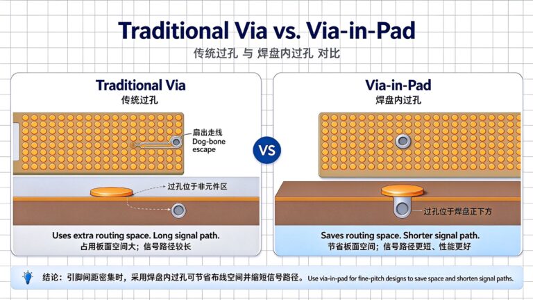
Traditional vias sit in the non-component areas of a PCB. The Via-in-Pad (VIP) technique places the via directly on an SMD pad and then plates it. The diagram below compares VIP with traditional vias.
1.How It Works
To build VIP, designers deposit conductive material—usually copper—inside a plated through hole (PTH), then cover it with a solder mask. The pad and the via then connect directly. The board no longer needs separate traces or vias to link the pad to other areas. VIP shrinks the board, shortens signal paths, and improves signal performance.
1.1 Comparison with Traditional PTHs
Traditional PTHs, by contrast, pass through the non-component areas of the PCB and connect to traces on the other side. PTHs have long been the industry standard for through-hole technology. They remain widely used because they are reliable and easy to manufacture.
1.2 Manufacturing and Selection
Manufacturing VIP is demanding. It requires precise drilling and plating, and it usually costs more than traditional PTHs. Choose VIP or traditional PTHs based on the specific requirements of your PCB design and manufacturing process.
2. Background: Why VIP Emerged
Electronics keep becoming lighter, thinner, and smaller. PCBs therefore move toward higher density and greater complexity. This trend pushes chip makers to package chips at finer pitches—for example, QFNs, BGAs, and flip chips. To keep routes routable and protect signal integrity, designers adopt VIPPO structures. They combine VIPPO with classic methods such as dog-bone routing, micro-vias, skip vias, and pad-with-trace routing, and so achieve high-quality PCB designs.
3. Designing Via-in-Pad
When You Do Not Need VIP
Designers must fan out components before PCB routing so the inner layers can be reached. For BGA components whose fan-out lands between the solder pads, you do not need a VIP structure. Set the BGA fan-out parameters as follows: via diameter 0.15–0.2 mm, trace width 3–4 mil, and annular ring width 0.3–0.4 mm. BGA pin pitch must therefore exceed 0.35 mm for normal fan-out.
When You Need VIP
Set the via diameter before you fan out the BGA. Otherwise, the wrong via diameter prevents effective fan-out. When the BGA pin pitch is too small to fan out on the pad, design VIP structures to route on the inner layers or on the bottom layer.
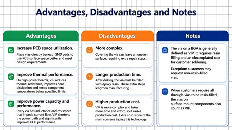
4. Advantages and Disadvantages
Decide whether to use VIP after weighing its pros and cons. Designers should evaluate the project against actual conditions before adopting this technology.
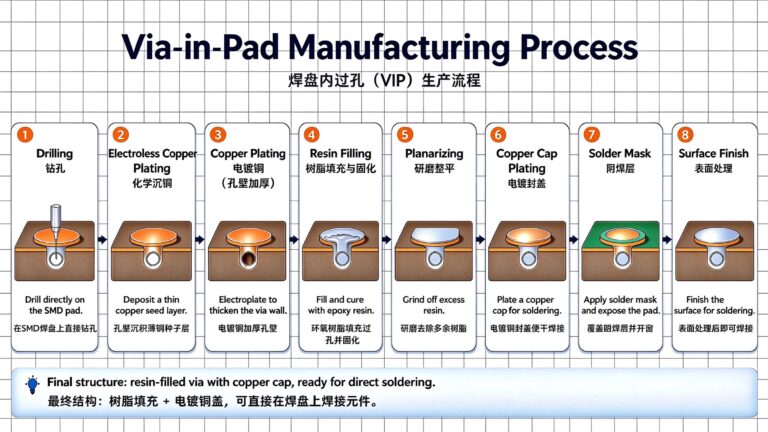
5.Via-in-Pad (VIP) Manufacturing Process
This image outlines the 8-step production flow for Via-in-Pad (VIP). PCB manufacturers use this technique for HDI boards. It allows engineers to place vias directly inside SMD pads. This saves space and creates a flat surface for soldering.
Here is how the factory builds it:
1.Drilling: The machine drills a hole directly into the SMD pad.
2.Electroless Copper Plating: The process deposits a thin copper seed layer on the hole walls.
3.Copper Plating: The factory electroplates the via to thicken the copper walls. This ensures a strong electrical connection.
4.Resin Filling: Workers fill the hole with epoxy resin and cure it. This stops solder from leaking through during assembly.
5.Planarizing: The grinder removes excess resin. This step makes the pad surface perfectly flat.
6.Copper Cap Plating: The line plates a new copper cap over the resin. This seals the hole and rebuilds the metal pad.
7.Solder Mask: The printer applies the green solder mask and exposes the pad.
8.Surface Finish: The factory adds the final surface finish (e.g., ENIG). This prevents oxidation and prepares the pad for soldering.
The Result: You get a flat, resin-filled via with a solid copper cap. Your assembly team can now solder components directly onto this pad.