Close Form
Menu


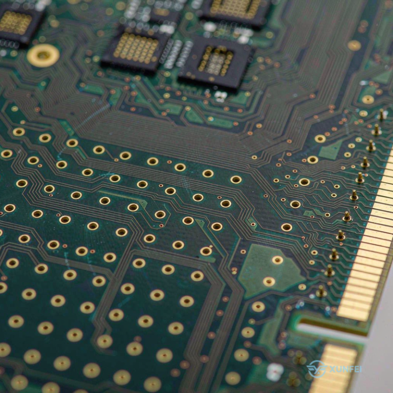
A PCB, or printed circuit board, is a board that mechanically supports electronic components and electrically connects them through patterned copper conductors. Instead of wiring every connection by hand, a PCB builds the circuit paths into a compact, repeatable structure. That is why computers, smartphones, vehicles, industrial equipment, medical devices, and household appliances all rely on PCBs.
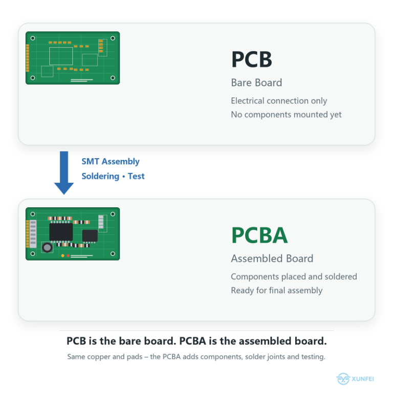
A bare PCB is not yet a finished electronic product. It is the manufactured board, complete with conductive patterns, pads, holes, and protective layers. Once components are mounted and soldered, the board becomes a printed circuit board assembly, or PCBA. This distinction matters when you request a quotation, because PCB fabrication and PCB assembly are related but separate services.
Most rigid PCBs use FR-4, a glass-fiber-reinforced epoxy laminate. FR-4 balances mechanical strength, electrical insulation, thermal performance, and cost. Applications such as high-frequency, flexible, rigid-flex, metal-core, and ceramic boards call for other materials.
Copper foil forms the conductive layer. During fabrication, the manufacturer removes unwanted copper and keeps the traces, planes, and pads that carry power and signals. A board may have one copper layer, two copper layers, or multiple inner and outer layers. Multilayer construction increases routing capacity, but it also demands tighter registration and stricter process control.
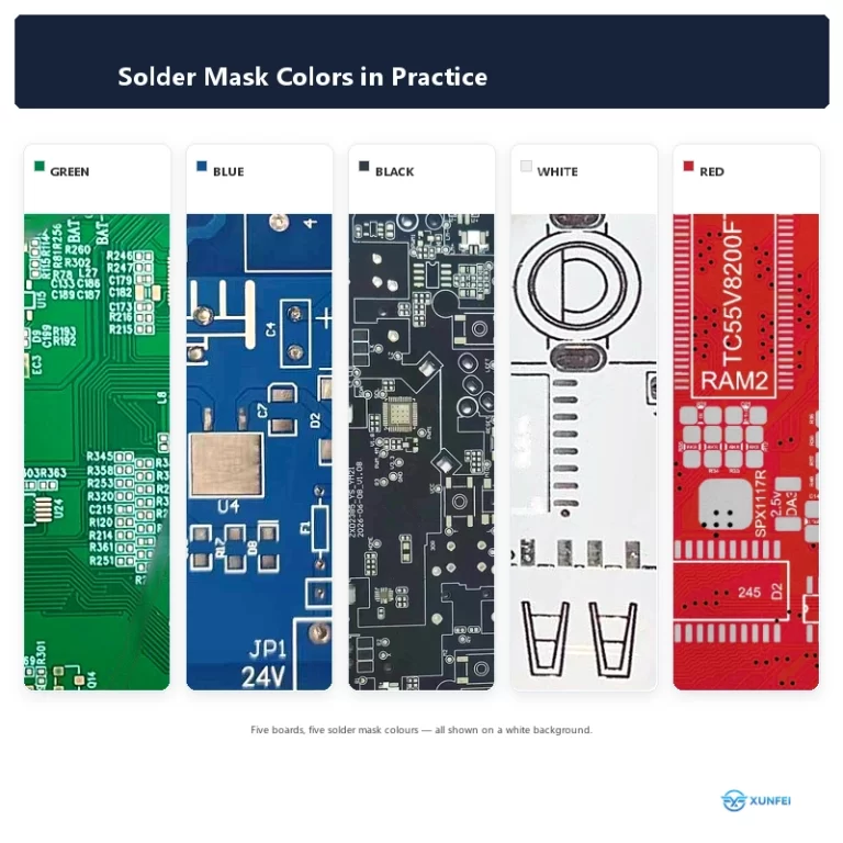
The solder mask is a protective insulating coating that covers most copper areas. It reduces accidental solder bridges and shields exposed copper from oxidation and contamination. Green is the most common color, and red, blue, black, and white are also available. The silkscreen carries reference designators, polarity marks, logos, and assembly notes. Surface finishes such as HASL and ENIG protect exposed pads and support reliable soldering.
Vias are plated holes that connect copper layers. Through vias run through the whole board, while blind and buried vias connect selected layers in more advanced designs. In practice, you should choose the stackup, material, copper thickness, impedance requirement, and surface finish as one package, based on electrical, mechanical, thermal, and manufacturing needs.
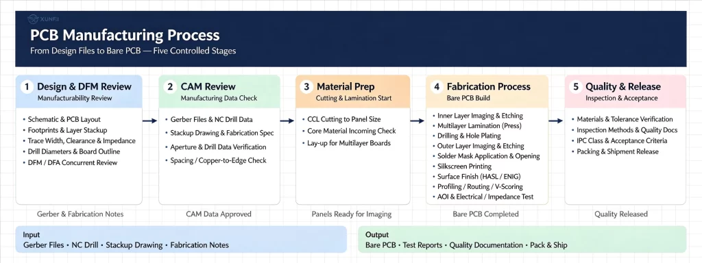
PCB manufacturing normally begins with a schematic and a PCB layout. The design team defines component footprints, layer stackup, trace widths, clearances, controlled-impedance rules, drill diameters, and board outline dimensions. The team should also review design for manufacturability and design for assembly before releasing the files.
The finalized layout then becomes manufacturing data, which normally includes Gerber files, NC drill files, a stackup drawing, and fabrication notes. The manufacturer runs a CAM review to catch problems, such as missing apertures, incorrect drill data, insufficient spacing, or conflicts between copper and board edges.
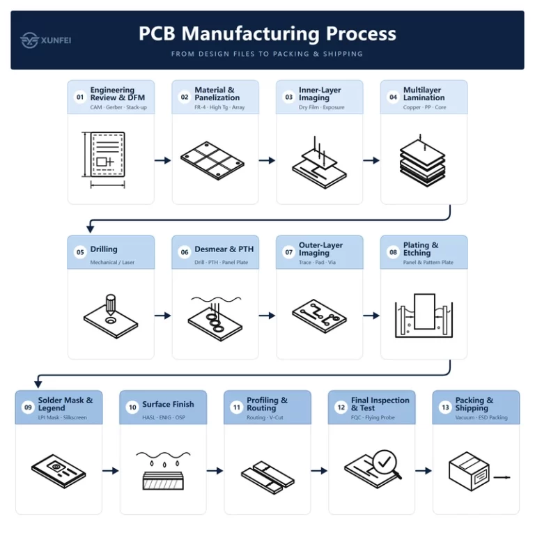
Fabrication may include imaging, etching, lamination for multilayer boards, drilling, hole plating, solder mask application, silkscreen printing, surface finishing, routing, and electrical testing. The exact sequence depends on the board type and the supplier's capability. A prototype may follow a different process from high-volume production, so keeping the two processes as close as possible lowers the transfer risk.
A professional PCB manufacturer should explain its materials, tolerances, inspection methods, accepted file formats, and quality documentation. IPC design and fabrication standards provide a widely used reference framework for consistent board requirements. Even so, you and your supplier should agree on the applicable class and acceptance criteria before production.
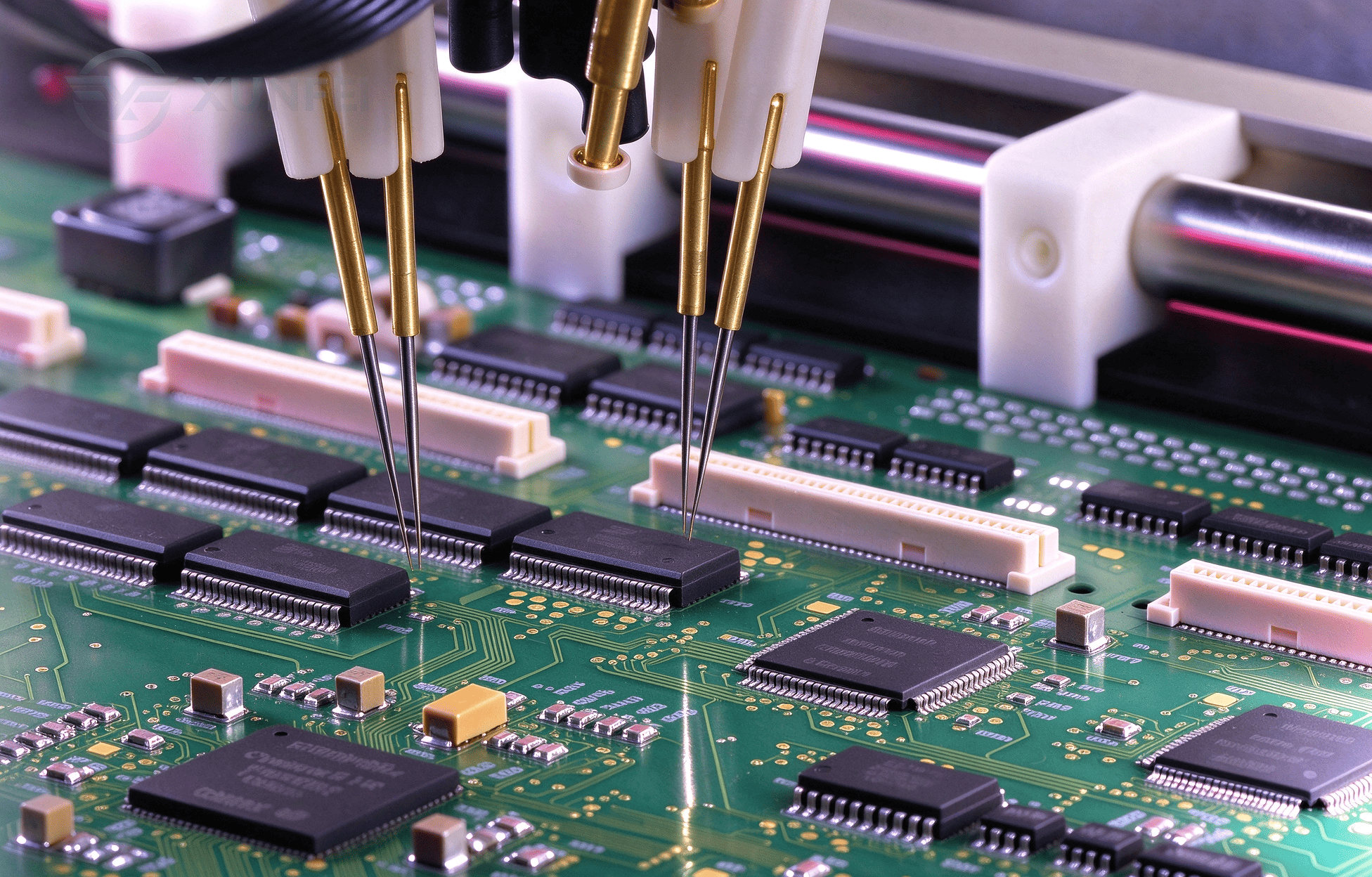
PCB assembly means mounting electronic components onto a fabricated board and forming reliable solder joints. SMT PCB assembly places surface-mount devices directly on the pads. The standard sequence includes solder paste printing, solder paste inspection, automated pick-and-place, reflow soldering, and inspection such as AOI or X-ray when needed.
Through-hole technology inserts component leads through drilled holes. It suits connectors, power components, mechanically stressed parts, and designs that need robust lead anchoring. Many products combine SMT and through-hole assembly, and the industry calls this mixed or hybrid assembly.
The assembly process depends on accurate component data. A typical production package includes the BOM, the centroid or pick-and-place file, assembly drawings, PCB fabrication files, approved part numbers, and special process instructions. Missing or inconsistent data can cause delays, unplanned substitutions, placement faults, and avoidable cost overruns.
A professional PCB assembly service should connect fabrication, component sourcing, assembly, inspection, and final testing. Price alone, however, does not define the right partner. The right service matches the board's package density, component risk, quality requirement, schedule, and production volume.
PCB assembly design is not only about fitting components onto a board. It must also support reliable placement, soldering, inspection, heat dissipation, electrical performance, and future servicing. Component orientation, courtyard clearance, pad geometry, fiducials, thermal relief, and access for inspection all affect the yield. For that reason, designers should review every assembly detail before the layout is finalized.
DFM verifies that the board can be fabricated consistently. DFA verifies that the assembly team can place and solder every component efficiently. High-speed products also depend on signal integrity, return paths, impedance control, and electromagnetic compatibility. Power products, in turn, depend on copper width, thermal vias, heat spreading, and component temperature.
Custom PCB assembly becomes more predictable when the supplier reviews the design before quoting. Ask for feedback on part availability, alternate components, panelization, stencil design, minimum spacing, solder mask openings, test points, and programming requirements. Catching an issue at the design stage is usually far cheaper than correcting a board after production.
When you compare PCB assembly suppliers, start with capability instead of marketing claims. Check whether the supplier supports your board type, layer count, materials, package sizes, fine-pitch devices, BGA inspection, through-hole work, conformal coating, programming, and functional testing.
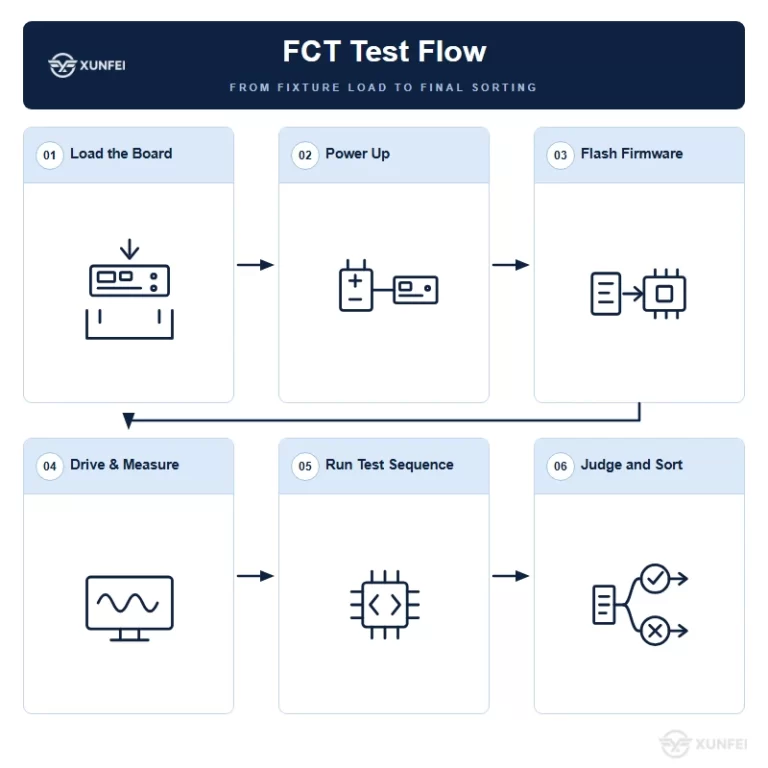
Next, evaluate quality control. A credible supplier should explain incoming inspection, component traceability, solder paste control, reflow profiling, AOI, X-ray when needed, electrical testing, nonconformance handling, and final documentation. Ask which IPC or customer-specific requirements the supplier follows, and how it approves deviations.
Then assess communication and supply-chain discipline. A high-quality PCB assembly partner should flag obsolete parts, long-lead items, minimum order quantities, and possible substitutions before you purchase. Clear revision control is essential, because an old BOM or an outdated Gerber file can trigger an expensive production error.
Finally, compare total project value. The lowest unit price is not always the lowest total cost, because scrap, delays, poor traceability, and repeated engineering changes quickly add up. A dependable supplier provides a clear quotation, a realistic schedule, review comments, production updates, and a defined support process.
A complete PCB assembly and manufacturing workflow can cover design review, bare-board fabrication, component sourcing, assembly, inspection, programming, testing, and delivery. This integrated model reduces handoffs and gives the customer one technical point of contact.
For a prototype, speed of learning matters most. The supplier should help identify design risks, verify the first assembled board, and document every change. For small-batch production, material continuity, repeatable setup, and traceability become more important. For volume production, panelization, cycle time, yield, change control, and supply continuity deserve closer attention.
A one-stop solution does not remove the customer's responsibility. The customer still approves the BOM, critical components, drawings, acceptance criteria, and engineering changes. The supplier provides manufacturing feedback and evidence that the agreed requirements are met. This shared responsibility creates a more reliable path from R&D to shipment.
8.FAQ
-What does PCB stand for?
PCB stands for printed circuit board. It is the physical platform that supports electronic components and provides conductive paths between them.
-What is the difference between PCB and PCBA?
A PCB is the fabricated bare board. A PCBA is that same board after you mount and solder electronic components onto it.
-What files are needed for PCB manufacturing?
Common files include Gerber data, NC drill files, stackup information, board drawings, fabrication notes, and the required material and finish specifications.
-Is SMT assembly better than through-hole assembly?
Neither is universally better. SMT is compact and efficient for many products, while through-hole assembly provides strong mechanical anchoring. A mixed process is often the most practical choice.
-How can I get a custom PCB assembly quotation?
Prepare the Gerber files, BOM, pick-and-place file, assembly drawings, quantity, target schedule, testing requirements, and any approved alternates. The supplier can then review the package, identify manufacturing risks, and send a quotation.
-What makes a reliable PCB assembly supplier?
A reliable supplier combines suitable equipment, documented quality control, component traceability, engineering feedback, transparent communication, and the ability to support both prototypes and volume production.
A PCB is more than a green board. It is a carefully engineered system of materials, copper geometry, insulation, holes, finishes, and manufacturing data. Understanding the difference between bare-board fabrication and assembly makes it easier to define requirements, compare suppliers, and prevent avoidable production problems.
Your project may need a prototype, a custom PCB assembly, or a complete PCB assembly and manufacturing program. Whatever the scale, the strongest results come from early design review, complete documentation, appropriate testing, and a supplier whose capabilities match the product's real requirements.Get your free quote.